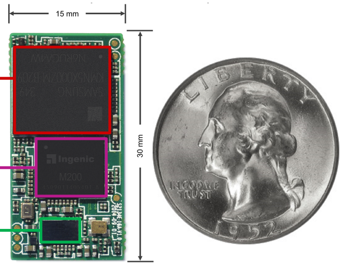
The wearables and IoT market are moving very quickly, and only seven months after announcing their Newton platform, Ingenic is following up with Newton2. This pace reminds me of the glory days of consumer graphics cards, when NVIDIA and ATI were clawing for market share and would each produce two large launches per year. While the PC (and even smartphone) market has matured to a slower pace, the wearables and IoT market is currently quite frenetic. Dozens of companies worldwide are attempting to cash in on the explosive growth potential. Over time, we will see consolidation as contenders are crowned champions, but who those champions will be is anyone’s guess at the moment.
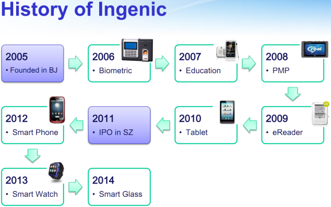
Ingenic is a relatively low profile company that could use an introduction. Ingenic is focused on semiconductors and devices and was founded in Beijing, China in 2005. Ingenic has licensed the MIPS architecture and designs their own CPU core and SoCs, and those designs are popular in low-end products such as digital picture frames, portable media players, and GPS devices. Ingenic had its IPO in 2011 and currently has a market cap of roughly $550 million.

Before getting to the details of Newton2, it’s important to understand positioning. Unlike other competitors, Ingenic positions the Newton (and Newton2) platform not as reference designs but instead as complete solutions. Ingenic would love to simply sell you the entire module as-is in high volume. However, Ingenic will build customized versions if you buy enough of them. This is similar to the Original Device Manufacturer (ODM) model, but in this case Newton is not an entire device but simply the electronics module. The purchaser still needs to place it into a full-fledged device like a smart watch or refrigerator. While Ingenic will sell you its custom designed SoCs as well, I am sure they would rather sell Newton as the margins for an integrated platform are guaranteed to be higher.
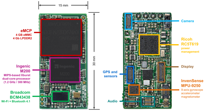
Now to the details. The Newton2 platform is a highly integrated module. These types of electronics are often referred to as a System on Module or SOM. Newton2 integrates the necessities of a wearable or IoT device, such as several built-in sensors and connectors for optional or obviously external components such as a display. Both Newton and Newton2 contain full featured application processors and can run Android.

| Ingenic Newton2 SOM | |||||||||||
| Size | 15mm x 30mm x 2.4mm | ||||||||||
| SoC | Ingenic M200 | ||||||||||
| Memory | 512MB LPDDR2 | ||||||||||
| Storage | 4GB eMMC | ||||||||||
| WiFi | Broadcom 43438 single-band 2.4GHz IEEE 802.11b/g/n | ||||||||||
| PMIC | Ricoh RC5T619 power management IC | ||||||||||
| Bluetooth | 4.1 | ||||||||||
| Sensor | IvenSense MPU-9250 gyroscope, accelerometer, magnetometer | ||||||||||
| Interfaces | Display, Capacitive Touch, DMIC and AOHPL/R Audio, MIPI-CSI or I2C Camera, UART, I2C, GPIO, RF 2.4 GHz antenna, USB 2.0 | ||||||||||
| Software | Android 4.4 | ||||||||||
Power consumption for Newton is 4mW standby, 100mW average, and 260mW peak. Newton2 claims to cut standby consumption to 3mW.
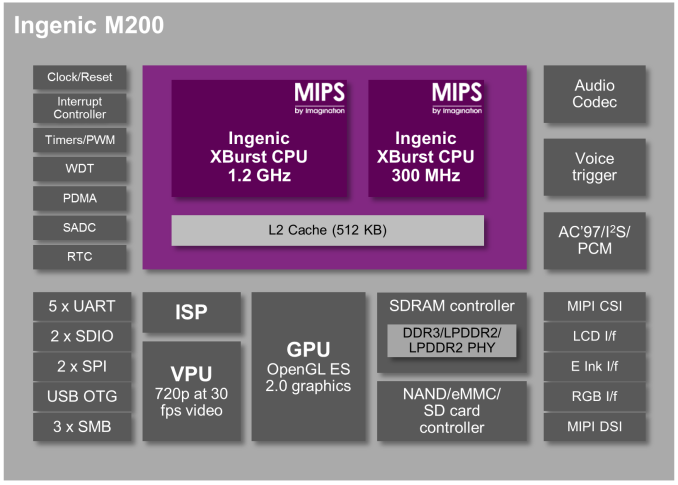
The SoC on Newton2 is entirely new, the Ingenic M200. Notable inclusions in M200, beyond the bevy of traditional functionality, are the LCD and E-Ink display controllers, voice trigger processing offload, and the M200 SoC.

| Ingenic M200 SoC | |||||||||||
| Package | BGA270, 7.7mm x 8.9mm x 0.76mm, 0.4mm pitch | ||||||||||
| CPU | XBurst1-HP core, 1.2 GHz XBurst1-LP core, 300 MHz |
||||||||||
| GPU | 2D/3D acceleration with OpenGL ES 2.0/1.1. OpenVG 1.1 | ||||||||||
| VPU | Video encoder up to 720p @ 30fps: H.264, VP8 Video decoder up to 720p @ 30fps: H.264, VP8, MPEG-1/2/4, VC-1, RV9 |
||||||||||
| ISP | HDR, video and image stabilization, crop and rescale, auto exposure + gain + white balance + focus control, edge sharpening, noise reduction, color correction, contrast enhancement, gamma correction | ||||||||||
| Memory | DDR2, DDR3, LPDDR, LPDDR2 up to 667 Mbps 64-bit ECC NAND flash support Toggle 1.0 and ONFI2.0 |
||||||||||
| Display | LCD controller with OSD: TFT, SLCD and MIPI-DSI (2-lanes) E-Ink controller |
||||||||||
| Camera | MIPI-CSI2 (2-lanes), DVP | ||||||||||
| Audio | Audio CODEC with 24-bit ADC/DAC, stereo line-in, MIC in, and headphone interface Low power DMIC controller AC97/I2S/SPDIF interface for external audio codec One PCM interface, supports both master and slave modes Voice trigger engine to wake system by programmable specific voice |
||||||||||
| ADC | 3 channels 12-bit SAR | ||||||||||
| Interfaces | USB 2.0 OTG x 1 MMC/SD/SDIO controller x 2 Full-duplex UART port x 5 Synchronous serial interface x 2 Two-wire SMB serial interface x 4 |
||||||||||
| Software | Android 4.4 | ||||||||||
Keep in mind that not every M200 interface is exposed on the Newton2. For example, accessing all five UARTs would require integrating the M200 into your own custom board.
The CPUs inside the M200 SOC set this SOM apart. The M200 integrates two custom designed Ingenic XBurst1 processors using the MIPS32 Release 2 ISA and include floating point and SIMD. Each processor is a full applications processor (AP) with an MMU and caches. However, you can consider the M200’s CPUs heterogeneous as one CPU is performance optimized and operates at up to 1.2 GHz while the other is optimized for power consumption and runs at up to 300 MHz. This is something we have seen before from NVIDIA with their Tegra devices as well as ARM's big.LITTLE, but it's different than other wearable and IoT efforts where low power duties are handled by a simple microcontroller (MCU). Using two APs likely simplifies software development somewhat, even if they are different, as they aren’t as enormously different as an AP and an MCU.
| XBurst1 CPU | |||||||||||
| Pipeline | 9-stage, single issue | ||||||||||
| Ingenic Estimated Performance |
2.0 DMIPS/MHz | ||||||||||
| ISA | MIPS32 Release 2 (both Integer and Floating Point ISA) XBurst SIMD |
||||||||||
| MMU | 32 dual-entry full associative joint TLB 4 entry ITLB 4 entry DTLB |
||||||||||
| L1 Cache | 32KB or 64KB I$ and D$ | ||||||||||
| L2 Cache | 256KB or 512KB | ||||||||||
| Debug | EJTAG | ||||||||||
| Process | 180nm, 90nm, 65nm, 40nm | ||||||||||
| Ingenic Estimated Power Consumption |
(1.0GHz, 0.09mW/MHz) @65nmLP (1.2GHz, 0.07mW/MHz) @40nmLP, performance optimized (500MHz, 0.05mW/MHz) @40nmLP, power optimized |
||||||||||
Looking at the XBurst1 power consumption, these cores are significantly lower power than the Cortex-A5 which ARM specifies at 0.12 mW/MHz on the same 40nm LP process. Comparing these cores beyond their power consumption is outside the scope of this article, but it is worth pointing out because ARM is citing Cortex-A5 as their most power efficient wearable CPU.
The XBurst1 CPU core has been around since 2005, when Ingenic was founded. Ingenic revealed in 2013 it had purchased a MIPS64 license and was developing XBurst2 with design completion targeted at 2014. This will go hand in hand with Android 5.0 supporting MIPS64 ISA natively. Keeping with their roughly six month pace, it isn’t too farfetched to imagine a Newton3 platform sporting a MIPS64 XBurst2 with Android 5.0 launching in mid-2015.
 MediaTek to Add NVIDIA G-Sync Support to Monitor Scalers, Make G-Sync Displays More Accessible
Qualcomm Adds Snapdragon 7s Gen 3: Mid-Tier Snapdragon Gets Cortex-A720 Treatment
- CXL Gathers Momentum at FMS 2024
- Fadu's FC5161 SSD Controller Breaks Cover in Western Digital's PCIe Gen5 Enterprise Drives
- PCI-SIG Demonstrates PCIe 6.0 Interoperability at FMS 2024
- DapuStor and Memblaze Target Global Expansion with State-of-the-Art Enterprise SSDs
- Phison Enterprise SSDs at FMS 2024: Pascari Branding and Accelerating AI
- Intel Sells Its Arm Shares, Reduces Stakes in Other Companies
- G.Skill Intros Low Latency DDR5 Memory Modules: CL30 at 6400 MT/s
- Samsung's 128 TB-Class BM1743 Enterprise SSD Displayed at FMS 2024
- Kioxia Demonstrates Optical Interface SSDs for Data Centers


2 Comments
View All Comments
link
Very cool to see this posted on AnandTech. I'm working on a project where we're looking at the Newton platform as a jumping-off point for a new design.Although the Newton2 is very interesting, the original Newton1, I think, is even more so. It's bigger, but it has everything you'd possibly want integrated into the design - audio amplifiers, every sensor under the sun, you name it.
But one thing that the article didn't get into - you can buy the Newton1 or Newton2 as a devkit, but you cannot buy the modules wholesale. So this isn't truly a SoM - it isn't meant to buy off the shelf and integrate into a product. It's meant to be a reference design that you can either copy, or tweak, or modify in to suit.
In other words, with Newton, you're still going to need to have someone manufacture and assemble PCBs, and it'll require a normal (and expensive, unpleasant) certification process. A true SoM would come pre-certified, making that process a lot easier (you still need to do a certification, but one one that's much less rigorous and costs a lot less).
Ingenic is definitely a company to watch, and they're making very smart moves. I'll have my own Newton1 in hand in a day or two, very exciting.
link
Hello hirschma, any thoughts on the newton 2, now that it's 9 months later? We are also looking at this. Your feedback is much appreciated. Thanks.